- 您现在的位置:买卖IC网 > Sheet目录317 > CAT24AA01WI-GT3 (ON Semiconductor)IC EEPROM SERIAL 1KB I2C 8SOIC
�� �
�
�CAT24AA01,� CAT24AA02�
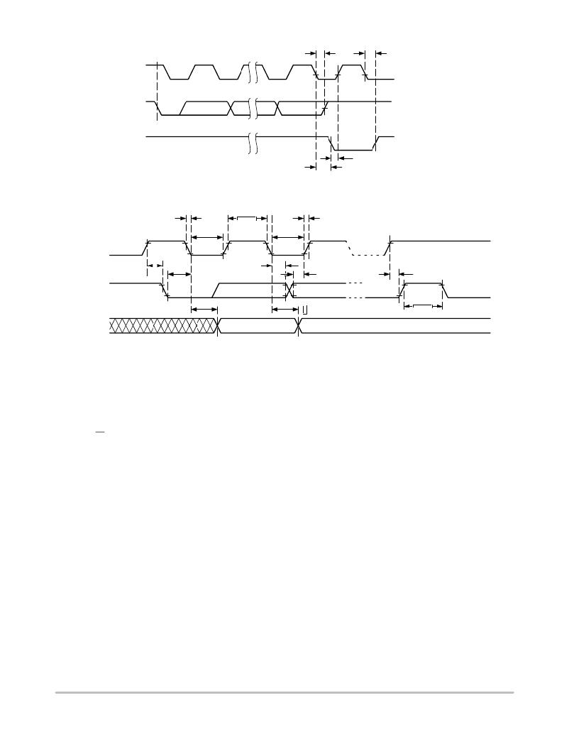
�BUS� RELEASE� DELAY� (TRANSMITTER)�
�BUS� RELEASE� DELAY� (RECEIVER)�
�SCL� FROM�
�MASTER�
�1�
�8�
�9�
�DATA� OUTPUT�
�FROM� TRANSMITTER�
�DATA� OUTPUT�
�FROM� RECEIVER�
�START�
�ACK� DELAY� (� ≤� t� AA� )�
�Figure� 4.� Acknowledge� Timing�
�ACK� SETUP� (� ≥� t� SU:DAT� )�
�SCL�
�t� F�
�t� LOW�
�t� HIGH�
�t� LOW�
�t� R�
�t� SU:STA�
�t� HD:STA�
�t� HD:DAT�
�t� SU:DAT�
�t� SU:STO�
�SDA� IN�
�t� AA�
�t� DH�
�t� BUF�
�SDA� OUT�
�Figure� 5.� Bus� Timing�
�WRITE� OPERATIONS�
�Byte� Write�
�To� write� data� to� memory,� the� Master� creates� a� START�
�condition� o� n� the� bus� and� then� broadcasts� a� Slave� address�
�with� the� R/W� bit� set� to� ‘0’.� The� Master� then� sends� an� address�
�byte� and� a� data� byte� and� concludes� the� session� by� creating�
�a� STOP� condition� on� the� bus.� The� Slave� responds� with� ACK�
�after� every� byte� sent� by� the� Master� (Figure� 5).� The� STOP�
�starts� the� internal� Write� cycle,� and� while� this� operation� is� in�
�progress� (t� WR� ),� the� SDA� output� is� tri� ?� stated� and� the� Slave�
�does� not� acknowledge� the� Master� (Figure� 6).�
�Page� Write�
�The� Byte� Write� operation� can� be� expanded� to� Page� Write,�
�by� sending� more� than� one� data� byte� to� the� Slave� before�
�issuing� the� STOP� condition� (Figure� 7).� Up� to� 16� distinct� data�
�bytes� can� be� loaded� into� the� internal� Page� Write� Buffer�
�starting� at� the� address� provided� by� the� Master.� The� page�
�address� is� latched,� and� as� long� as� the� Master� keeps� sending�
�data,� the� internal� byte� address� is� incremented� up� to� the� end�
�of� page,� where� it� then� wraps� around� (within� the� page).� New�
�data� can� therefore� replace� data� loaded� earlier.� Following� the�
�Acknowledge� Polling�
�As� soon� (and� as� long)� as� internal� Write� is� in� progress,� the�
�Slave� will� not� acknowledge� the� Master.� This� feature� enables�
�the� Master� to� immediately� follow� ?� up� with� a� new� Read� or�
�Write� request,� rather� than� wait� for� the� maximum� speci� ?� ed�
�Write� time� (t� WR� )� to� elapse.� Upon� receiving� a� NoACK�
�response� from� the� Slave,� the� Master� simply� repeats� the�
�request� until� the� Slave� responds� with� ACK.�
�Hardware� Write� Protection�
�With� the� WP� pin� held� HIGH,� the� entire� memory� is�
�protected� against� Write� operations.� If� the� WP� pin� is� left�
�?� oating� or� is� grounded,� it� has� no� impact� on� the� Write�
�operation.� The� state� of� the� WP� pin� is� strobed� on� the� last�
�falling� edge� of� SCL� immediately� preceding� the� 1� st� data� byte�
�(Figure� 8).� If� the� WP� pin� is� HIGH� during� the� strobe� interval,�
�the� Slave� will� not� acknowledge� the� data� byte� and� the� Write�
�request� will� be� rejected.�
�Delivery� State�
�The� CAT24AA01/02� is� shipped� erased,� i.e.,� all� bytes� are� FFh.�
�STOP,� data� loaded� during� the� Page� Write� session� will� be�
�written� to� memory� in� a� single� internal� Write� cycle� (t� WR� ).�
�http://onsemi.com�
�5�
�发布紧急采购,3分钟左右您将得到回复。
相关PDF资料
CAT24AA02WI-G
IC EEPROM SERIAL 2KB I2C 8SOIC
CAT24C01ZI-G
IC EEPROM SERIAL 1KB I2C 8MSOP
CAT24C03WI-G
IC EEPROM SERIAL 2KB I2C 8SOIC
CAT24C04ZI-G
IC EEPROM SERIAL 4KB I2C 8MSOP
CAT24C05YI-G
IC EEPROM SERIAL 4KB I2C 8TSSOP
CAT24C08TDI-GT3
8KB I2C SER EEPROM TSOT 23
CAT24C128HU4IGT3
IC EEPROM 128KB I2C SRL 8UDFN
CAT24C164YI-G
IC EEPROM SERIAL 16KB I2C 8TSSOP
相关代理商/技术参数
CAT24AA01WI-T
制造商:CATALYST 制造商全称:Catalyst Semiconductor 功能描述:1-Kb and 2-Kb I2C CMOS Serial EEPROM
CAT24AA01WI-T10
制造商:ONSEMI 制造商全称:ON Semiconductor 功能描述:1-Kb and 2-Kb I2C CMOS Serial EEPROM
CAT24AA01WI-T3
制造商:ONSEMI 制造商全称:ON Semiconductor 功能描述:1-Kb and 2-Kb I2C CMOS Serial EEPROM
CAT24AA02
制造商:ONSEMI 制造商全称:ON Semiconductor 功能描述:1-Kb and 2-Kb I2C CMOS Serial EEPROM
CAT24AA02TDI-10
制造商:CATALYST 制造商全称:Catalyst Semiconductor 功能描述:1-Kb and 2-Kb I2C CMOS Serial EEPROM
CAT24AA02TDI-3
制造商:CATALYST 制造商全称:Catalyst Semiconductor 功能描述:1-Kb and 2-Kb I2C CMOS Serial EEPROM
CAT24AA02TDI-G10
制造商:CATALYST 制造商全称:Catalyst Semiconductor 功能描述:1-Kb and 2-Kb I2C CMOS Serial EEPROM
CAT24AA02TDI-G3
制造商:CATALYST 制造商全称:Catalyst Semiconductor 功能描述:1-Kb and 2-Kb I2C CMOS Serial EEPROM